Sunday 22 September 2013

REGISTER SET OF 8086 MICROPROCESSOR

Registers:

Most of the registers contain data/instruction offsets within 64 KB memory segment. There are four different 64 KB segments for instructions, stack, data and extra data. To specify where in 1 MB of processor memory these 4 segments are located the 8086 microprocessor uses four segment registers: 

Code segment (CS) is a 16-bit register containing address of 64 KB segment with processor instructions. The processor uses CS segment for all accesses to instructions referenced by instruction pointer (IP) register. CS register cannot be changed directly. The CS register is automatically updated during far jump, far call and far return instructions. 

Monday 2 September 2013


The Intel 8255A is a general purpose programmable I/O device which is
designed for use with all Intel and most other microprocessors.It provides 24 I/O pins which may be individually programmed in 2 groups of 1 and used in 3 major modes of operation.The 8255 is a 40 pin integrated circuit (IC), designed The 8255 is a 40 pin It designed by Intel for the 8080 microprocessor
Two control groups, labeled group A control and group B control define how the three I/O ports operate. There are several different operating modes for the 8255 and these modes must be defined by the CPU writing programming or control words to the device 8255.
The line group of port C consists of two 4 bit ports. One of the 4 bit group is associated with group A control and the other 4 bit group with group B control device signals. The upper 4 bits of port C are associated with group A control while the lower 4 bits are associated with group B control.
The final logic blocks are read/write control logic and data bus buffer. These blocks provide the electrical interface between the Z80 and the 8255.
The data bus buffer buffers the data I/O lines to/from the Z80 data bus. The read/write control logic routes the data to and from the correct internal registers with the right timing. The internal path being enabled depends on the type of operation performed by the Z80. The type of operation can be I/O read or I/O write.

Tuesday 14 May 2013

Bus Interface Unit (BIU):-
  This unit contains following parts of 8086:-
  • 6 byte instruction queue
  • segment registers (CS,DS,ES,SS)
  • instruction  pointer

 This unit performs following steps:-
  •  Instruction fetch, Instruction queuing, Operand fetch and storage, Address relocation and Bus control.
  • The BIU uses a mechanism known as an instruction stream queue to implement a pipeline architecture
  • This queue permits prefetch of up to six bytes of instruction code. When ever the queue of the BIU is not full, it has room for at least two more bytes and at the same time the EU is not requesting it to read or write operands from memory, the BIU is free to look ahead in the program by prefetching the next sequential instruction.
  •  These prefetching instructions are held in its FIFO queue.With its 16 bit data bus, the BIU fetches two instructionbytes in a single memory cycle.
  •  After a byte is loaded at the input end of the queue, itautomatically shifts up through the FIFO to the emptylocation nearest the output.
  • The EU accesses the queue from the output end. It readsone instruction byte after the other from the output of thequeue. If the queue is full and the EU is not requestingaccess to operand in memory.
  •  These intervals of no bus activity, which may occur between bus cycles are known as Idle state.
  •  If the BIU is already in the process of fetching an instruction when the EU request it to read or write operands from memory or I/O, the BIU first completes the instruction fetch bus cycle before initiating the operand read / write cycle
  • The BIU also contains a dedicated adder which is used to generate the 20 bit physical address that is output on the address bus. This address is formed by adding an appended 16 bit segment address and a 16 bit offset address.
  •  For example, the physical address of the next instruction to be fetched is formed by combining the current contents of the code segment CS register and the current contents of the instruction pointer IP register.
  • The BIU is also responsible for generating bus control signals such as those for memory read or write and I/O read or write.

8086 microprocessor:-

 The microprocessor 8086 belongs from the group of 16-bit microprocessor chip designed by Intel between early 1976 and mid-1978. it have data bus of 16- bit and address bus of 20-bit. it have memory of 1MB power supply of +5v. CPU clock rate is 5MHz to 10MHz. it have package of 40 pin IC. it have eight general purpose register including stack pointer base pointer and source index and destination index. four segment register and a program counter. it have 9 flag register.

  • microprocessor- 16bit
  • data bus           - 16bit
  • address bus      - 20bit
  • power supply   - +5v
  • CPU clock rate- 5MHz to 10MHz
  • package           - 40 pin IC
  • memory           - 1MB

Block diagram of 8086:- 


It contains two parts EU and BIU.


Execution unit(EU):- this unit performs following steps.


  • Decodes instructions fetched by BIU
  • Generate control signals
  • Executes instruction    


This unit contains 8 general purpose register
  1. Accumulator register AX- AH and AL
  2. Base register  BX- BH and BL
  3. Count register CX- CH and CL
  4. Data register   DX- DH and DL
  5. SP- stack pointer
  6. BP- base pointer
  7. SI-  source index
  8. DI- destination index   
Register AX,BX,CX and DX is of 16-bit each but it is devided into two registers high and low of 8-bit for each register. and we can use as  8-bit or 16-bit. two pointers are stack pointer and base pointer and two index registers are source index and destination index.

Arithmetic logic unit (ALU):- this unit performs arithmetic and logic operation.

Execution and control system:- this unit performs the process of execution and controls all the process of execution unit.

Flag register:- a flag is a flip flop which indicates some condition produced by the execution of an instruction. 8086 have nine 16-bit flag registers.

  1. carry flag
  2. sign flag
  3. parity flag
  4. auxiliary flag
  5. zero flag
  6. overflow flag
  7. interrupt flag
  8. direction flag
  9. trap flag
it have five same flag register like 8085 and four different flag registers are overflow flag, interrupt flag, direction flag and trap flag.


Functions of execution unit:-
  • The Execution unit is responsible for decoding and executing all instructions.
  • The EU extracts instructions from the top of the queue in the BIU, decodes them, generates operands if necessary, passes them to the BIU and requests it to perform the read or write by cycles to memory or I/O and perform the operation specified by the instruction on the operands.
  •  During the execution of the instruction, the EU tests the status and control flags and updates them based on the results of executing the instruction.
  • If the queue is empty, the EU waits for the next instruction byte to be fetched and shifted to top of the queue.
  •  When the EU executes a branch or jump instruction, it transfers control to a location corresponding to another set of sequential instructions.
  • Whenever this happens, the BIU automatically resets the queue and then begins to fetch instructions from this new location to refill the queue.


Saturday 11 May 2013

ADDRESSING MODES:

The method by which address of source of the data or destination of the data is given in the instruction is called addressing modes. the way in which address of the data is specified in 
instruction is known as addressing modes

8085 uses five types of addressing modes.
  1. Direct addressing mode
  2. Register addressing mode 
  3. Register indirect addressing mode
  4. Immediate addressing mode
  5. Implicit addressing mode
Direct addressing mode:-  In this mode addressing, address of the operand is given in
 instruction itself.

       example: LDA 2500 H,
It load the content of memory location 2500 H in to accumulator.
  •  LDA  is the operation
  • 2500 H is source of data
  • accumulator is destination
 
Register addressing mode :- In this mode of addressing, operand is in general purpose

    register.
     
     example: MOV A , B
It transfer the data of register B in to accumulator. 
  • MOV is operation.
  • register B is source of data
  • accumulator is destination

Register indirect addressing mode:- In this mode of addressing , address of  operand is specified
 register pair.

    example: MOV A, M
 It transfer the data from memory specified by H-L pair of register to accumulator.
  • MOV is operation
  • memory is source.
  • accumulator is destination.

Immediate addressing mode
:- In this mode of addressing operand is specified within the

 instruction itself.

example: MVI A , 05 H
It  move data 05 H into accumulator.
  • MVI is operation
  • 05 H is source.
  • accumulator is destination.

Implicit addressing mode
:- In this mode of addressing address of source of data as well as

 address of destination of is fixed. 'means no need of operand in instruction' called implicit mode.

example: CMA
Complement accumulator.
  • CMA is operation
  • accumulator is source
  • accumulator is destination.

Wednesday 8 May 2013

INSTRUCTION SET: 

An instruction set is a command given to the computer to perform specific operation. it contains command , operand and address of source  and destination.

8085 Microprocessor have five types of instruction set :  

  • Data transfer instruction

  • Arithmetic  instructions

  • Logical instructions

  • Control instructions

  • Branching instructions 

    Data transfer instructions:   Instructions, which are used to transfer data from one register to another register, from memory to register or register to memory, come under this group. Examples are: MOV, MVI, LXI, LDA, STA etc. When an instruction of data transfer group is executed, data is transferred from the source to the destination without altering the contents of the source.


    • MOV r1, r2 (Move Data; Move the content of the one register to another).  [r1] <-- [r2]
    • MOV r, m (Move the content of memory register). r <-- [M]
    • MOV M, r. (Move the content of register to memory). M <-- [r]
    • MVI r, data. (Move immediate data to register). [r] <-- data.
    • MVI M, data. (Move immediate data to memory). M <-- data.
    • LXI rp, data 16. (Load register pair immediate). [rp] <-- data 16 bits, [rh] <-- 8 LSBs of data.
    • LDA addr. (Load Accumulator direct). [A] <-- [addr].
    •  STA addr. (Store accumulator direct). [addr] <-- [A].
    • LHLD addr. (Load H-L pair direct). [L] <-- [addr], [H] <-- [addr+1].
    • SHLD addr. (Store H-L pair direct) [addr] <-- [L], [addr+1] <-- [H].
    • LDAX rp. (LOAD accumulator indirect) [A] <-- [[rp]]
    • STAX rp. (Store accumulator indirect) [[rp]] <-- [A].
    • XCHG. (Exchange the contents of H-L with D-E pair) [H-L] <-->  [D-E].


     Arithmetic instructions:  The instructions of this group perform arithmetic operations such as addition, subtraction; increment or decrement of the content of a register or memory. Examples are: ADD, SUB, INR, DAD etc.


    •  ADD r. (Add register to accumulator) [A] <-- [A] + [r].DAA (Decimal adjust accumulator) .
    • ADD M. (Add memory to accumulator) [A] <-- [A] + [[H-L]].
    • ADC r. (Add register with carry to accumulator). [A] <-- [A] + [r] + [CS].
    • ADC M. (Add memory with carry to accumulator) [A] <-- [A] + [[H-L]] [CS].
    • ADI data (Add immediate data to accumulator) [A] <-- [A] + data.
    • ACI data (Add with carry immediate data to accumulator). [A] <-- [A] + data + [CS].
    • DAD rp. (Add register paid to H-L pair). [H-L] <-- [H-L] + [rp].
    • SUB r. (Subtract register from accumulator). [A] <-- [A] – [r].
    • SUB M. (Subtract memory from accumulator). [A] <-- [A] – [[H-L]].
    • SBB r. (Subtract register from accumulator with borrow). [A] <-- [A] – [r] – [CS].
    • SBB M. (Subtract memory from accumulator with borrow). [A] <-- [A] – [[H-L]] – [CS].
    • SUI data. (Subtract immediate data from accumulator) [A] <-- [A] – data.
    • SBI data. (Subtract immediate data from accumulator with borrow). [A] <-- [A] – data – [CS].
    • INR r (Increment register content) [r] <-- [r] +1.
    • INR M. (Increment memory content) [[H-L]] <-- [[H-L]] + 1.
    • DCR r. (Decrement register content). [r] <-- [r] – 1.
    • DCR M. (Decrement memory content) [[H-L]] <-- [[H-L]] – 1.
    • INX rp. (Increment register pair) [rp] <-- [rp] – 1.
    • DCX rp (Decrement register pair) [rp] <-- [rp] -1.


    Logical instructions: The Instructions under this group perform logical operation such as AND, OR, compare, rotate etc. Examples are: ANA, XRA, ORA, CMP, and RAL etc.

    • ANA r. (AND register with accumulator) [A] <-- [A] ^ [r].
    • ANA M. (AND memory with accumulator). [A] <-- [A] ^ [[H-L]].
    • ANI data. (AND immediate data with accumulator) [A] <-- [A] ^ data.
    • ORA r. (OR register with accumulator) [A] <-- [A] v [r].
    • ORA M. (OR memory with accumulator) [A] <-- [A] v [[H-L]]
    • ORI data. (OR immediate data with accumulator) [A] <-- [A] v data.
    • XRA r. (EXCLUSIVE – OR register with accumulator) [A] <-- [A] v   [r]
    • XRA M. (EXCLUSIVE-OR memory with accumulator) [A] <-- [A] v  [[H-L]]
    • XRI data. (EXCLUSIVE-OR immediate data with accumulator) [A] <-- [A]
    • CMA. (Complement the accumulator) [A] <-- [A]
    • CMC. (Complement the carry status) [CS] <-- [CS]
    • STC. (Set carry status) [CS] <-- 1.
    • CMP r. (Compare register with accumulator) [A] – [r]
    • CMP M. (Compare memory with accumulator) [A] – [[H-L]]
    • CPI data. (Compare immediate data with accumulator) [A] – data.The 2nd byte of the instruction is data, and it is subtracted from the content of the accumulator. The status flags are set according to the result of subtraction. But the result is discarded. The content of the accumulator remains unchanged.
    • RLC (Rotate accumulator left) [An+1] <-- [An], [A0] <-- [A7],[CS] <-- [A7].
      The content of the accumulator is rotated left by one bit. The seventh bit of the accumulator is moved to carry bit as well as to the zero bit of the accumulator. Only CS flag is affected.
    • RRC. (Rotate accumulator right) [A7] <-- [A0], [CS] <-- [A0], [An] <-- [An+1].
      The content of the accumulator is rotated right by one bit. The zero bit of the accumulator is moved to the seventh bit as well as to carry bit. Only CS flag is affected.
    • RAL. (Rotate accumulator left through carry) [An+1] <-- [An], [CS] <-- [A7], [A0] <-- [CS].
    • RAR. (Rotate accumulator right through carry) [An] <-- [An+1], [CS] <-- [A0], [A7] <-- [CS]

  • Branching instructios:  This group includes the instructions for conditional and unconditional jump, subroutine call and return, and restart. Examples are: JMP, JC, JZ, CALL, CZ, RST etc.

    • JMP addr (label). (Unconditional jump: jump to the instruction specified by the address). [PC] <-- Label.
    • Conditional Jump addr (label): After the execution of the conditional jump instruction the program jumps to the instruction specified by the address (label) if the specified condition is fulfilled. The program proceeds further in the normal sequence if the specified condition is not fulfilled. If the condition is true and program jumps to the specified label, the execution of a conditional jump takes 3 machine cycles: 10 states. If condition is not true, only 2 machine cycles; 7 states are required for the execution of the instruction.
      • JZ addr (label). (Jump if the result is zero)
      • JNZ addr (label) (Jump if the result is not zero)
      • JC addr (label). (Jump if there is a carry)
      • JNC addr (label). (Jump if there is no carry)
      • JP addr (label). (Jump if the result is plus)
      • JM addr (label). (Jump if the result is minus)
      • JPE addr (label) (Jump if even parity)
      • JPO addr (label) (Jump if odd parity)
    • CALL addr (label) (Unconditional CALL: call the subroutine identified by the operand)CALL instruction is used to call a subroutine. Before the control is transferred to the subroutine, the address of the next instruction of the main program is saved in the stack. The content of the stack pointer is decremented by two to indicate the new stack top. Then the program jumps to subroutine starting at address specified by the label.
    • RET (Return from subroutine)
    • RST n (Restart) Restart is a one-word CALL instruction. The content of the program counter is saved in the stack. The program jumps to the instruction starting at restart location.

  •  Control instructions:   This group includes the instructions for input/output ports, stack and machine control. Examples are: IN, OUT, PUSH, POP, and HLT etc


    • IN port-address. (Input to accumulator from I/O port) [A] <-- [Port]
    • OUT port-address (Output from accumulator to I/O port) [Port] <-- [A]
    • PUSH rp (Push the content of register pair to stack)
    • PUSH PSW (PUSH Processor Status Word)
    • POP rp (Pop the content of register pair, which was saved, from the stack)
    • POP PSW (Pop Processor Status Word)
    • HLT (Halt)
    • XTHL (Exchange stack-top with H-L)
    • SPHL (Move the contents of H-L pair to stack pointer)
    • EI (Enable Interrupts)
    • DI (Disable Interrupts)
    • SIM (Set Interrupt Masks)
    • RIM (Read Interrupt Masks)
    • NOP (No Operation)


REGISTER SET OF 8085:

  • 8085 have six general purpose register to store 8- bit data during execution.
  • these registers are B,C,D,E,H and L.
  • they can combine to perform 16-bit operation and denoted as BC,DE and HL pair.  
ACCUMULATOR(A) :
  • The accumulator is an 8-bit register .
  • This register is a part of ALU unit
  • This register is used to store 8-bit data and to perform arithmetic and  logic operation.
  • The result of an operation is stored in accumulator
FLAG REGISTER:-
  • flag register are used to test data condition.
  • 8085 have five flag register of 8-bit.
  • these are following: Zero flag(Z), Sign flag(S), Carry flag(CY), Parity flag(P) and Auxiliary flag(AU)
Sign flag(S):  After execution of any arithmetic and logic operation, if the result of D7 is 1,sign flag is set otherwise reset.
Zero flag(S): If the result of arithmetic or logic operation is zero then it is set otherwise reset.

Carry flag(CY): If any arithmetic and logic operation produce any carry then carry flag is set otherwise reset.
Parity flag(P): If result of any arithmetic and logic operation contains even no of 1's then it is set otherwise reset.
Auxiliary carry flag(AU): When D3 generates any carry during arithmetic and logic operation then it is set otherwise reset.


ARITHMETIC LOGIC UNIT (ALU):

  • It is used to perform arithmetic operation like (addition, subtraction, multiplication and division) and logic operation like (AND, OR and EX-OR etc)
  • It receives data from accumulator and registors.
  • According to results it set or reset the flags.
PROGRAM COUNTER (PC)

  • This 16-bit register deals with sequencing the execution of instructions. 
  • This register is a memory pointer. Memory locations have 16-bit addresses, and that is why this is a 16-bit register.
  • The microprocessor uses this register to sequence the execution of the instructions.The function of the program counter is to point to the memory address from which the next byte is to be fetched. When a byte (machine code) is being fetched, the program counter is incremented by one to point to the next memory location  
STACK POINTER (SP)
  • The stack pointer is also a 16-bit register used as a memory pointer. 
  • It points to a memory location in R/W memory, called the stack. 
  • The beginning of the stack is defined by loading 16-bit address in the stack pointer. 
INSTRUCTION  REGISTER/DECODER:

Temporary store for the current instruction of a program. Latest instruction sent here from memory prior to execution. Decoder then takes instruction and ‘decodes’ or interprets the instruction. Decoded instruction then passed to next stage.

Memory Address Register:  Holds address, received from PC, of next program instruction. Feeds the address bus with addresses of location of the program under execution.

Control Generator:  Generates signals within uP to carry out the instruction which has been decoded. In reality causes certain connections between blocks of the uP to be opened or closed, so that data goes where it is required, and so that ALU operations occur.

Register Selector  This block controls the use of the register stack in the example. Just a logic circuit which switches between different registers in the set will receive instructions from Control Unit.

General Purpose Registers  uP requires extra registers for versatility. Can be used to store additional data during a program. More complex processors may have a variety of differently named registers. 

Timing and Control unit:

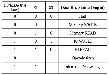
  • It has three control signals ALE, RD (Active low) and WR (Active low) and three status signals IO/M(Active low), S0 and S1

  • ALE is used for provide control signal to synchronize the components of microprocessor and timing for instruction to perform the operation. 

  • RD (Active low) and WR (Active low) are used to indicate whether the operation is reading the data from memory or writing the data into memory respectively.
  • IO/M(Active low) is used to indicate whether the operation is belongs to the memory or peripherals.


Monday 6 May 2013

The functional block diagram or architecture of 8085 Microprocessor is very important as it gives the complete details about a Microprocessor.


 Fig. shows the Block diagram of a Microprocessor.


8085 BUS STRUCTURE
 address bus:-
  • The address bus is a group of 16 lines generally identified as A0 to A15. 
  • The address bus is unidirectional: bits flow in one direction-from the MPU to peripheral devices.
  • The MPU uses the address bus to perform the first function: identifying a peripheral or a memory location.  

DATA BUS:-
  • The data bus is a group of eight lines used for data flow.
  • These lines are bi-directional - data flow in both directions between the MPU and memory and peripheral devices.
  • The MPU uses the data bus to perform the second function: transferring binary information.
  • The eight data lines enable the MPU to manipulate 8-bit data ranging from 00 to FF (28 = 256 numbers).
  • The largest number that can appear on the data bus is 11111111

 Control bus:-
  • The control bus carries synchronization signals and providing timing signals.
  • The MPU generates specific control signals for every operation it performs. These signals are used to identify a device type with which the MPU wants to communicate.


DMA Request Signal:
HOLD and HLDA:-HOLD is an active high input signal used by the other controller to request microprocessor about use of address, data and control signal. The HOLD and HLDA signal are used for direct memory access(DMA). DMA controller receives a requests from a device and in turn issues the HOLD signal to the microprocessor.
The processor releases the system bus and then acknowledges the HOLD signal with HLDA signal. The DMA transfer thus begins.


logic schematic diagram of 8085
Serial Input Output port:-
SID and SOD:-These pins are used for serial data communication.


Introduction:-


Today the microprocessor based products have revolutionized every area of human  activity and have made a deep impact on quality of life. Right from small chip to supercomputer Microprocessor have become an integral part of the system. Microprocessor evolved from the developments in computer. One such microprocessor is Intel’s 8085, which is most popularly used and regarded as a basic microprocessor. The microprocessors operation can be described through the organization of computer model.

Generally a computer organization is as follows

INPUT> ALU+CONTROL UNIT+MEMORY> OUTPUT
      (1)                           (2)                                                  (3)

Unit 2 is generally replaced with microprocessor. So a microprocessor can be represented as :
Microprocessor=ALU+Registers+Program Counter+Control and Timing circuit+Stack Pointer +Interrupt Circuit.

PIN DIAGRAM:-

8085 is a general purpose microprocessor having 40 pins and works on single power supply. To study the pin diagram we group
 the signals into 6 categories:

1.Power Supply
2.Interrupt Signals
3.Address and Data bus
4.Control and Status signals
5.Serial I/O Port
6.DMA Request Signals


 Power supply and Clock frequency signals:


  • VCC:-Vcc is to be connected to +5V power supply.
  • Vss:-Ground reference
  • X1 and X2:- This pin is used for providing the clock frequency to the microprocessor. Generally Crystal oscillator or LC oscillator is used to generate the frequency.
  •  The frequency generated here is internally divided into two.As we know that the basic operating timing frequency of the microprocessor is 3 MHz so 6 MHz frquency is applied.
  • CLK (output)-Clock Output is used as the system clock for peripheral and devices interfaced with the microprocessor.

 Multiplexed Address / Data Bus:


  • AD0-AD7:-These are multiplexed address and data bus. So it can be used to carry the lower order 8 bit address as well as the data. Generally these lines are demultiplexed using the Latch.
  • During the opcode fetch operation, in the first clock cycle the lines deliever the lower order address bus  A0-A7.
  • In the subsequent IO/M read or write it is used as data bus D0-D7. CPU can read or write data through these lines.
  • A8-A15:- These are address bus used to address the memory location.

 Interrupt signal:

  • Pin 6 to 11:- These pins are used for interrupt signals. Generally and external devices are connected here which requests the microprocessor to perform a particular task.
  • There are 5 pins for hardware interrupts-
    TRAP, RST7.5, RST 6.5, RST5.5 and INTR
  • INTA is used for acknowledgement. Microprocessor sends the acknowledgement to external devices through the INTA pin. 

Control And Status Signal:

  • S0 and S1:-It is used for the status signal in microprocessor
  • .ALE(Airthmetic Latch Enable):-This signal is used to capture the lower address presented on multiplexed address and data bus.
  • RD:-This is active low input generally
     used for reading operation.
  • WR:-This is active low input used for writing operation.
  • IO/M:-This pin is used to select the memory or input-output through which we want to communicate the data.
  • READY:-As we know that memory and input -output have slower response than microprocessor. So a microprocessor may now be able to handle further data till it completes the present job. So it is in waiting state. As it completes the present job it sets the READY pin. Microprocessor enters into wait state while READY pin is disabled.
  • RESET IN:-This is active low input. This pin is used to reset the microprocessor. An active low signal applied to this pin reset the program counter inside the microprocessor. The busses are tristated.
  • RESETOUT:-If we want to reset the external devices connected to the microprocessor then a signal applied to this pin resets the external devices.